Introduction: Why PCB Files Matter
Whether you are trying to handover a design to your engineering team, understanding how to interface with your contract manufacturing vendors, or trying to resurrect an old project, sifting through Printed Circuit Board (PCB) files can be challenging for those that are not working in PCB design as their primary role.
Locating the full and complete file set is critical to ensure a design can be updated, fabricated, and assembled consistently.
PCB projects encompass various file types, each serving a specific role in communicating the design’s details. Here’s an overview of these file categories:
- Design Files: Files that are native to the Electronic Computer-Aided Design (ECAD) software to fully capture the PCB design, including schematics, layout, and other project files. These files are required for your engineering team, but typically not sent to manufacturers.
- Project File: Defines the overall configuration of the project and links all other files to the project.
- Schematic Files: Graphical representation of all components and connection.
- Library Files: Contains symbols and footprints used in the design.
- Other: CAD Drawing files (Altium Draftsman), Output job files, simulation, etc.
- PCB Fabrication files: Files required to build the unpopulated circuit board.
- Fabrication Drawings: Defines the major board dimensions, layer stack-up, fabrication notes.
- Gerbers or ODB++ Files: Sets of files to communicate the physical construction of the PCB.
- Drill file: Provides location and drill size for all holes on the PCB. Multiple drill files may be provided if there are both un-plated and plated holes.
- PCB Assembly Files: Files required to install components on to the PCB
- Pick & Place Files: Contains the location and orientation of each component, used for automated machine placement of components.
- Bill of Materials: Complete list of the components to be placed on the PCB, includes part numbers, descriptions, quantities, designators, and potential alternatives.
- Assembly Drawings: Contains information about any processes to be completed after components have been populated on a PCB.
PCB Design Files (Native ECAD Files)
Design files are created in Electronic Computer-Aided Design (ECAD) software and contain schematics, PCB layouts, and component libraries. These are used by engineers for editing, simulation, and generating manufacturing outputs but not typically sent to manufacturers.
Common ECAD Platforms
- Altium Designer
- Cadence OrCAD
- KiCad
- Eagle
- Siemens PADS
Each ECAD platform uses unique file extensions. Here’s a quick reference:
| File Type | Altium | OrCAD | KiCad | Eagle | PADS |
|---|---|---|---|---|---|
| Project File | .PrjPcb | .opj | .kicad_pro | .epf | .prj |
| Schematic | .SchDoc | .dsn | .kicad_sch | .sch | .sch |
| PCB Layout | .PcbDoc | .brd, .max | .kicad_pcb | .brd | .pcb |
| Symbol Library | .Schlib | .olb | .kicad_sym | .lbr | .c, .p |
| Footprint Library | .Pcblib | .psm, .pad | .kicad_mod | .lbr | .d |
Key Design File Types
- Project Files: Organize and link all schematic, layout, and output files
- Schematic Files: Represent circuit logic and electrical connections
- PCB Layout Files: Contain board dimensions, trace routing, and physical component placement
- Library Files: Define reusable component symbols (schematics) and footprints (PCB pads)
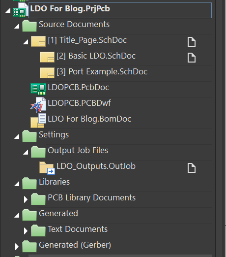
While libraries aren’t always required to open a completed project, they are vital for reuse and modification in future designs, interconnect schematic, PCB, and output files to ensure that every layer of the project is appropriately placed in the design. Here’s an example project structure in Altium Designer:
Library Files
Library files are used by ECAD software to match individual part number’s symbols to their footprint, allowing for reuse of common symbols and footprints throughout a project. These library files create the building blocks for schematics and PCB designs.
Component symbols are visual representations of the connections and functions of a component. Common standard passive components (resistors, diodes, capacitors) each have a unique identifying symbol that many will be familiar with, but individual integrated circuits (ICs) each require a unique symbol to be created for them.
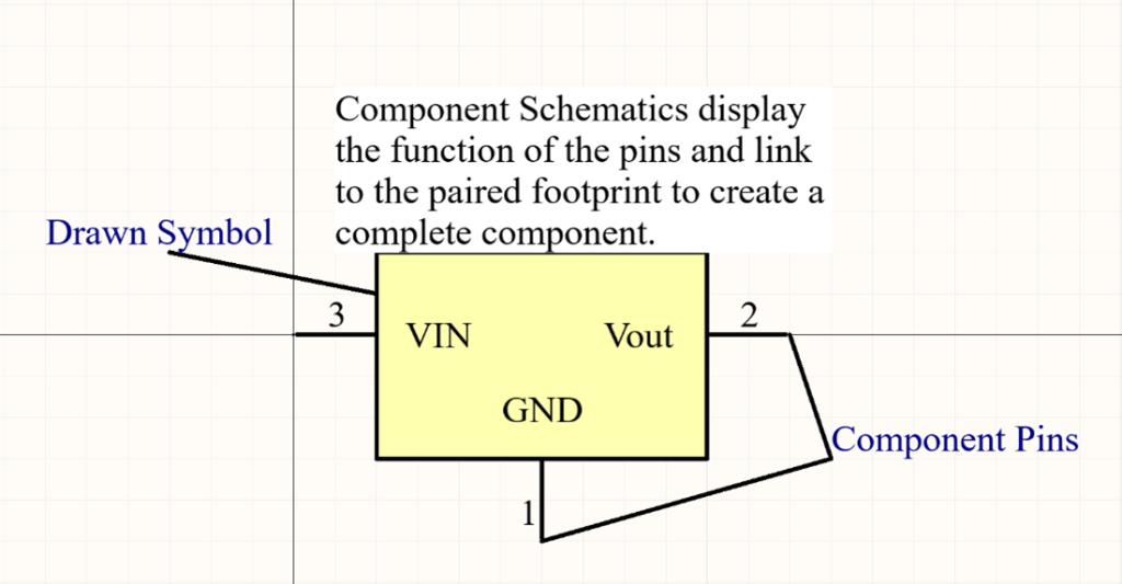
Component Footprint files are dimensioned visual representation of the pads for electrical components, these are placed within the PCB design to dictate the position and size of the exposed copper to solder components to.

Design Source Files
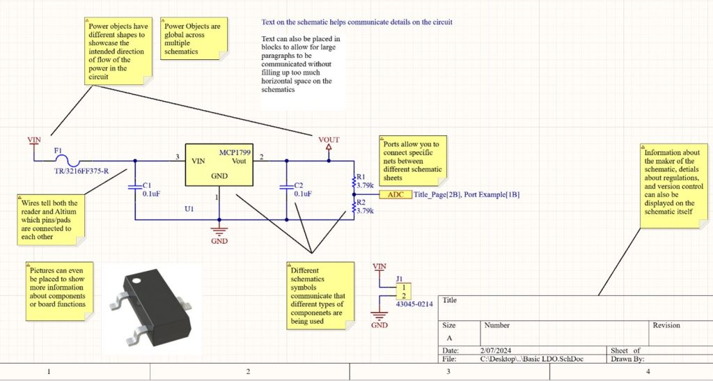
Schematics – Within ECAD software, schematics house the electrical design of the PCB and allow others reading them to understand how the PCB is intended to function.
PCB Layout – PCB layout files are dimensioned visual representations of the PCB, showing the physical sizing, stack up order, and routing within the design. Footprints are placed and connected throughout the design to generate fabrication files which manufactures can use to create PCBs.

PCB Fabrication Files
Manufacturers typically shouldn’t need the design files unless they’re also verifying the functionality of the PCBs with tests such as fly probe tests. Manufacturing files provide a PCB manufacturer with the details of the physical placement of fiberglass, conductors, and holes throughout a design allowing the bare PCB to be assembled. While assembly files inform them of special requirements that may be necessary during the build process such as potting locations or assembly orientations.
Gerbers and Drill Files
Gerber files (RS-274X format) describe individual PCB layers. While aging, they’re still widely accepted by manufacturers.
Common Gerber Extensions
- Copper Layers:
.GTL(Top),.GBL(Bottom),.G1,.G2(Inner) - Silkscreen:
.GTO(Top Overlay),.GBO(Bottom Overlay) - Solder Mask:
.GTS,.GBS - Paste Layers:
.GTP,.GBP - Board Outline/Mechanical:
.GKO,.GML,.GMx - Drills:
.DRL,.TXT,.PHO,.D,.ART
Use Altium CAM viewer (or other CAM tools) to validate your Gerber and drill files before sending to the fabricator.
ODB++ Files
ODB++ Files are a more modern file type and often preferred over Gerber files. ODB++ files contain more information than Gerbers. Check with your manufacturer on their file type preference between ODB++ and Gerbers.
ODB files are a large set of file often storred as a single .zip or .tgz comressed file. The compressed file typically contains folders such as fonts, input, matrix, misc, steps, symbols, each of which may contain many subfolders and files.
PCB Fabrication Drawing
To help ensure your PCB is built to specification, a pdf drawing should be provided with fabrication notes, layer stackup table, drill table, or other specific information about the desired quality of construction of the PCB. These drawings can often be created within the PCB layout itself and exported within the manufacturing files as well.
PCB Assembly Files
Your PCB Assembly contract manufacturer will need the Gerber or ODB++ files. In addition to those files, they will need a few other files.
Pick and Place
A pick and place file, or sometimes referred to as an “XY” file typically has a .txt extension and contains the X and Y coordinates and orientation of each component. This file is use for automated machine placement of parts on an assembly line.
Bill of Materials
The Bill of Materials should contain part numbers, description, reference designators, quantities, and other critical information such as approved alternate parts. This is often in .xlsx or .csv format.
PCB Assembly Drawing
The PCB Assembly Drawing is typically a PDF and would include notes required for assembly, such as special installation instructions, solder requirements, conformal coating instructions, and other critical details.
Conclusion: Start with the Right Files
For the best results in editing, manufacturing, and assembly, always work from native ECAD files when possible. Here’s a quick reference:
| Task | File Type |
|---|---|
| Design | .PrjPcb, .SchDoc, .PcbDoc |
| Manufacture | .GTL, .GBL, .DRL, or .ZIP ODB++ |
| Assemble | .TXT (PnP), .CSV (BOM), .PDF (Assembly Drawing) |
Understanding what each PCB file does — and when to use it — helps ensure your project moves forward without costly delays or confusion.
Help! I am Missing Files
If you’re missing critical files or only have a physical board, don’t panic.
At Sparx Engineering, we can:
- Reverse-engineer your design from a physical PCB
- Recreate missing schematic or layout files
- Update or modernize legacy designs
- Generate manufacturing-ready file sets
Contact us if you’re unsure what you need — we’ll help you sort it out.