Exploring One of the Most In-Demand Careers in Electronics
There are thousands of career paths out there — but as someone who’s built a profession around Printed Circuit Board (PCB) design, I can confidently say: becoming a PCB Designer is one of the most rewarding and in-demand careers today.From consumer electronics to AI infrastructure to electric vehicles and aerospace, nearly every modern innovation relies on well-designed PCBs. As global industries push toward smarter, smaller, faster, and more connected devices, the demand for skilled PCB Designers continues to grow rapidly.
What does a PCB Designer do?
The simple answer: PCB Designers design printed circuit boards.
The complete answer is much broader.
The short and sweet answer is they design PCBs (Printed Circuit Boards). The more in-depth answer is they design PCBs to fit a certain application and set of requirements for a customer to meet their customer’s need. They start by coming up with a circuit that fits their requirements and then use PCB design CAD tools to make schematics and PCB layouts to capture their circuit. Then they work with PCB fabrication shops and assembly shops to build the PCBs and put electrical parts on them. Once they get the assembled PCBs in hand, they test, troubleshoot, and reiterate until they have a circuit that meets their requirements. Below are some key aspects of a PCB Designer’s job and the image below shows the PCB design process flowing from problem identification to computer circuit design to finished PCB to integrating the PCB into a product to a final solution with real world impact. Just like an amputee receiving an advance prosthetic!

- E-CAD Tools: Designers find themselves getting really knowledgeable in electrical design concepts as well as skilled with PCB CAD software. Here’s an article of the Top PCB Design Softwares in use today. Altium and Cadence dominate in the professional design software industry, and KiCad is a great free, open-source software to get started learning how to design PCBs.
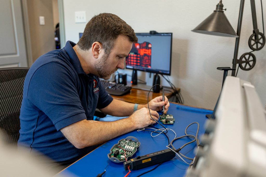
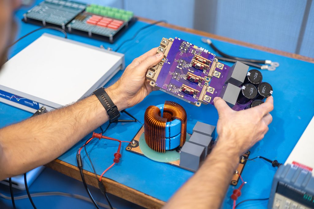
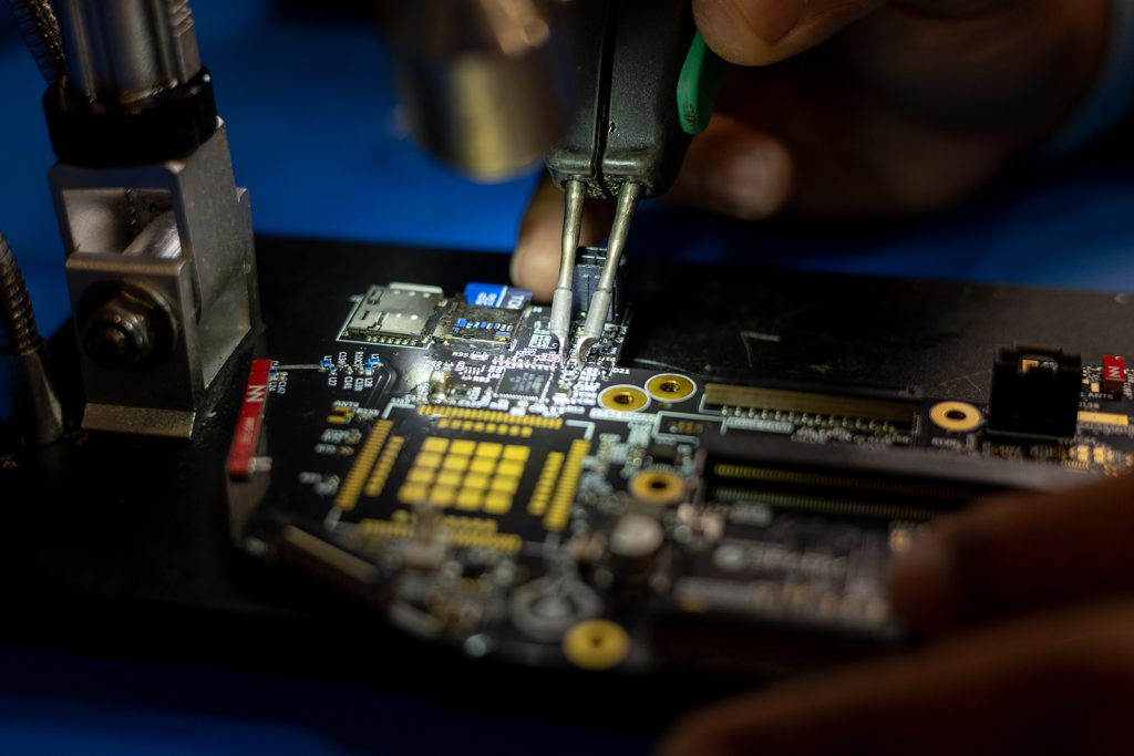
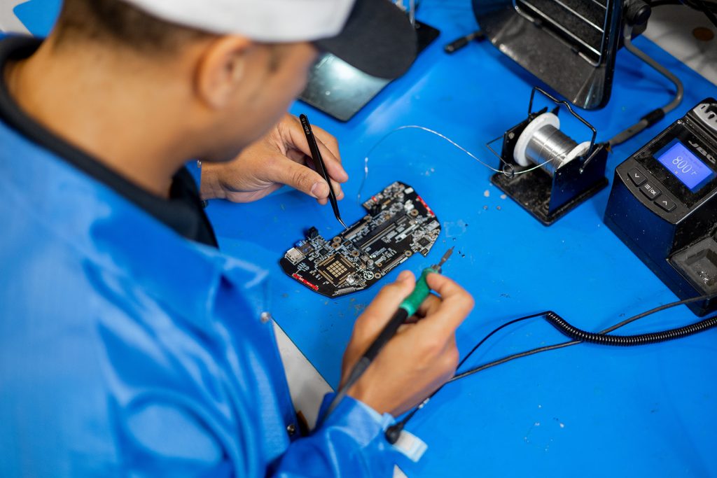
- Hands On: Design work is not always at a computer. Good designers have hands-on skills in soldering, inspecting electronics, working with test equipment, running wiring, and prototyping full devices.
- Cross-Discipline: PCB Designers will also work with other disciplines like software and mechanical engineering to make sure their design supports the software’s hardware needs and implements the right physical features to interface with the real world.
- Full Spectrum: PCB Designers can find themselves in one area of this process or all of it. This leads designers to have a very comprehensive view of the design and manufacturing process.
Where does a PCB Designer work?
Anywhere and everywhere. Every industry uses electronics; Medical, Oil & Gas, Aerospace, Military, Consumer Products, Industrial, Automotive, Underwater Applications, Robotics, Computers, Energy, Research, and the list goes on and on. Several online reports show there are about 10,000 PCB Designers in the US currently, but many more are needed to support the continual demand for a more electronic world. PCB designers also find themselves at a range of sizes of companies from huge international companies down to smaller local companies which again just shows that Designers are needed everywhere. The Bureau of Labor Statistics groups PCB Designers under Electrical & Electronics Engineering and gives promising projections for this field over the next decade.
What does it take to become a PCB Designer?
The main path is a Bachelor’s of Science degree in Electrical Engineering from a 4 year accredited University. Here you will learn all the fundamentals of electricity and get an intro to circuit design. (It’s really important that your degree is from an ABET accredited program so employers will recognize your degree and so that you can get licensed. You can look up ABET accredited engineering degree programs here.) Past that, real world experience in a junior engineering position and tinkering with electronics on your own will help build you into a competent designer. Just as the world of electronics is quickly growing so is the world of hobbyist electronics who document their projects and lessons learned online. There is no shortage of material to learn from and nerd out over. (Here are several great Youtube channels to learn from.) A Master’s or PhD in Electrical Engineering is not a requirement, but they only improve your knowledge base for PCB design. Additionally, pursuing your Professional Engineering (P.E.) license helps designers stay sharp out in the field. The rigorous study for the exams followed by continuing education every year afterwards promotes designers that are always growing and staying on top of modern electronics developments. This isn’t a requirement to become a PCB designer, but P.E.’s stand out among designers. Learn more about the licensure process here.
Key Skills of a Modern PCB Designer
ECAD Tools & Design Software
Designers become experts in tools like Altium Designer, Cadence OrCAD/Allegro, or open-source tools like KiCad. These platforms allow engineers to draw schematics, create PCB layouts, and export manufacturing files.
Hands-On Prototyping
PCB design isn’t just screen time. Great designers also:
-
Solder prototypes
-
Use multimeters, oscilloscopes, and logic analyzers
-
Build harnesses and wire assemblies
-
Physically inspect and debug real boards
Cross-Functional Collaboration
PCB Designers work with software, mechanical, and test engineers to ensure the circuit board mechanically fits, can properly run the firmware, and performs as expected.
Full Lifecycle Perspective
Designers often support the entire lifecycle. From concept to manufacturing to field support PCB designers give them deep insight into how their boards impact real products.
Why Sparx Engineering is a Great Place to Be a PCB Designer
At Sparx Engineering, our PCB Designers work across the full spectrum of the product development lifecycle — from blank-sheet concept to real-world integration.
Our team:
-
Uses industry-leading PCB CAD tools
-
Works with fabricators and assembly houses regularly
-
Prototypes, solders, and tests PCBs hands-on
-
Supports a wide range of industries and technologies
Whether you’re an engineer looking to expand your technical breadth or a business seeking high-reliability PCB development, Sparx Engineering provides the environment to push boundaries.
An Engineering Career with Real-World Impact
There’s lots of great reasons to become a PCB Designer, and at Sparx Engineering, our PCB Designers get to work the full spectrum of what a PCB Designer can do. A Sparx PCB Designer is well versed in PCB Design Software, has vast knowledge of the PCB fabrication & assembly process, and is experienced in troubleshooting, soldering, and testing. Sparx PCB Designers get this experience because Sparx designs for every industry and works with a wide range of technologies. Sparx is a great place for engineers who want a wide range of PCB design experience and for businesses in need of engineering support for their product’s PCB needs.
At Sparx Engineering, our PCB Designers gain experience across industries and technologies, building both technical depth and manufacturing expertise.
If you’re considering a career in electronics or need engineering support for your next product, PCB design is one of the most exciting and impactful paths available.