With the increasing popularity of Altium Designer in the electronics industry, many professionals and hobbyists are transitioning from other PCB design tools to Altium to take advantage of its advanced features and user-friendly interface. As a result, converting existing KiCad PCB files to Altium has become a common task. This blog will guide you through converting your KiCad PCB files to Altium, ensuring a smooth transition and helping you leverage the full potential of Altium’s powerful design capabilities.
Why Convert from KiCad to Altium
Altium Designer is renowned for its robust design tools, extensive library management, and superior integration with other engineering workflows. While KiCad is an excellent open-source tool, Altium provides a more polished user experience, better support, and advanced features such as interactive routing, 3D visualization, and design rule-checking. Transitioning to Altium can significantly enhance productivity and PCB quality.
Preparing for the Migration
Before you begin, consider why you need to import your data. Here are some common considerations:
- Do you have any critical data that must be preserved?
- Is it more efficient to start new designs rather than rework imported data?
- How will you verify the imported data?
- Do you need to leverage Altium specific features?
- How will you maintain library integrity and design authority?
Steps to Import KiCad Project into Altium Designer
1. Prepare Your KiCAD project:
Ensure all your KiCad files are organized and complete. You only need your .pro, .sch, and .kicad_pdb files to migrate from KiCad to Altium Designer. To convert models and components, .lib files are also needed. Here is a guide to the files needed for your import:
- KiCad pro Files (*.pro)
- KiCad kicad_pro Files (*.kicad_pro)
- KiCad sch Files (*.sch)
- KiCad kicad_sch Files (*.kicad_sch)
- KiCad kicad_pcb Files (*.kicad_pcb)
- KiCad lib Files (*.lib)
- KiCad kicad_sym Files (*.kicad_sym)
- KiCad kicad_mod Files (*.kicad_mod)
2. Open Altium Designer:
Launch Altium Designer on your computer.
3. Enable the KiCad Importer Extension
To use the KiCad Importer, ensure it is installed. Access the Extensions & Updates view by clicking the control at the top-right of the workspace, then choose Extensions and Updates from the menu. If the KiCad Importer extension is not listed, you will need to install it. Open the Purchased tab, find the KiCad Importer extension, and click to download it. Restart Altium Designer when prompted.
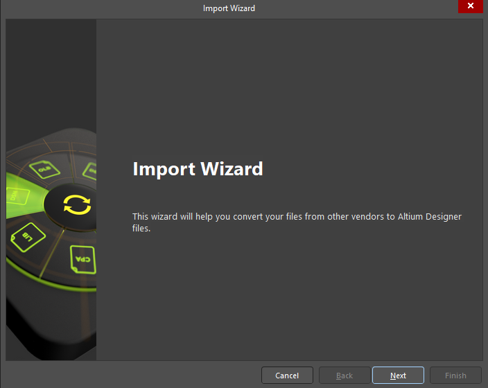
4. Importing the KiCad Project:
Go to File > Import Wizard. In the Import Wizard, select KiCad from the list of supported formats and click Next.
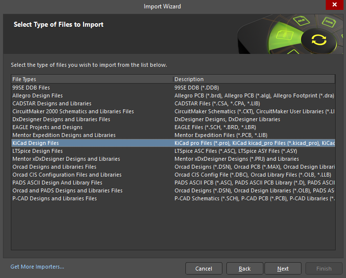
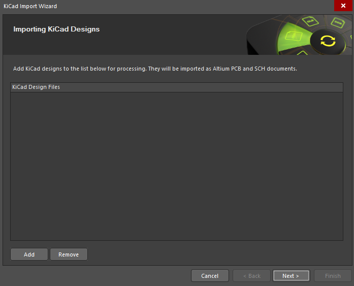
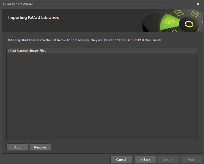
5. Select the KiCad Files:
Browse and select the KiCad schematic and PCB files you want to import. Make sure to select both the schematic (.sch) and PCB layout (.kicad_pcb) files.
6. Configure Import Options:
Review and configure the import options. Adjust settings based on your specific project requirements, such as handling of net names, design rules, and component footprints.
7. General Import Options:
Use the General Options dialog to set up general log reporting options. Enable options like Log All Errors, Log All Warnings, and Log All Events.
8. Log of Analyzing:
The Log of Analyzing dialog lists any errors/warnings found during the scanning of the KiCad files you are importing.
9. Review Output Project Structure:
Review the output project structure and specify the Output Directory where the files will be imported.
10. Schematic Import Options:
Set the import options for your schematic. Check the desired options.
11. PCB Import Options:
If the KiCad project includes a PCB, there will be additional PCB Import Options and Current Board Layer Mapping pages displayed. Complete these as required and click Next.
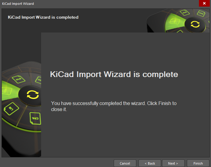
12. Complete the Import:
Once the above options have been specified, the Importing Progress page will display. When the progress bars reach 100%, the KiCad Import Wizard is completed. Click Finish in the Wizard to close it. The result of the import can be seen in the Projects panel.
Post Import Tidy Up
Once the import is complete, review the imported schematic and PCB layout in Altium Designer. Ensure everything is correctly translated and optimized for Altium’s environment. Here is a checklist of key checks:
- Physical Check
- Verify board shape and cutouts
- Electrical Check
- Verify netlist and design rules
- Rules
- Ensure all design rules have been imported
- Perform a design rule check
- Power Check
- Verify nets, planes, and polygons
- Documentation Check
- Ensure layers, text/strings, and legends are correctly imported
- Verify the number of components/nets and that all nets are routed
- Gerber Files Check
- Generate Gerber files for the imported project and view them with Altium’s Camtastic Viewer to ensure they are consistent with the KiCAD files.
Conclusion
Converting your KiCad project to Altium Designer can be straightforward with the right tools and steps. Altium’s Import Wizard makes the transition smooth, allowing you to take full advantage of Altium’s powerful features and improve your PCB design workflow. By following the steps outlined in this guide, you can ensure a successful conversion and start leveraging the benefits of Altium Designer for your future projects.
2 Responses
there are issues importing KiCad designs in version 10, the footprints do not automatically come over in the import you have to manually map the footprints, this is only in version 10 that this happens, hopefully Altium will do a fix for this soon.
This problem is a real pain. I might end up sticking with KiCAD and not migrating to Altium if this doesn’t get sorted out.